Sputtering Targets and Sputtered Films: Technology and Markets
April 14, 2008
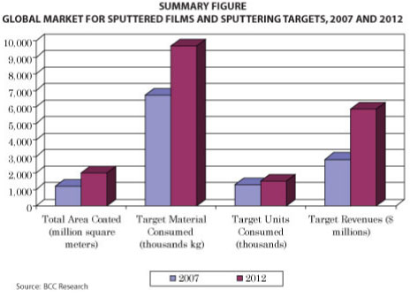
According to a new technical market research report, Sputtering Targets and Sputtered Films: Technology and Markets (SMC037D) from BCC Research, the global market for sputtered films and sputtering targets was worth $2.8 billion in 2007. This is expected to increase to $5.9 billion by 2012, a compound annual growth rate (CAGR) of 15.8%.
Nearly 1.3 million sputtering targets were consumed in 2007. This is expected to increase to more than 1.5 million targets in 2012, for a CAGR of 3.6%. In 2007 this amounted to 1,217.7 million square meters of thin films for semiconductors, passive components, recording heads, flat panel displays, data storage media, wear and corrosion resistant coatings, lubricant films, photovoltaic cells, automotive and architectural glass, biological coatings, and other applications. This is expected to increase to 1,980.2 million square meters by the end of 2012, for a CAGR of 10.2%.
The microelectronics sector historically has been the largest consumer of sputtering targets, but this will change by 2012. In the semiconductor industry, the ongoing transition to copper wiring, which uses electroplating as the major thin film deposition method, and the introduction of alternative manufacturing technologies to meet the miniaturization requirements established by the International Technology Roadmap for Semiconductors, will lead to reduced use of the sputtering process during the next 5 years.
Nevertheless, sales of sputtering targets are expected to grow at a very healthy rate, driven by the utilization of these products in the fabrication process of other fast growing applications, such as advanced displays and solar cells. Other factors that will positively affect the expansion of the sputtering target market include the availability of new target compositions for emerging applications, the availability of raw materials and process equipment, and the increasing market penetration of the sputtering process in developing countries.
Source: BCC Research
Sputtering Targets and Sputtered Films: Technology and Markets( SMC037D )
Publish Date: Apr 2008
Data and analysis extracted from this press release must be accompanied by a statement identifying BCC Research LLC as the source and publisher. For media inquiries, email press@bccresearch.com or visit www.bccresearch.com/media to request access to our library of market research.
BCC Library Membership Benefits
Unlimited Access to Market Research Reports for Academic Institutions and Corporations.
Custom Research
Tailored solutions across industries for your unique business needs.
Sputtering Targets and Sputtered Films: Technology and Markets
Customize This Report More in Semiconductors
- Global Flexible PCB Market to Nearly Double, Reaching $41.7 Billion by 2030 on Surging Demand from Consumer Electronics, EVs and 5G Infrastructure
- Semiconductor Silicon Wafer Market Set to Reach $20.2 Billion Globally by 2030
- BCC Research Forecasts 15.4% CAGR for Global Chip-on-Board LED Market Through 2030
- Semiconductor Chip Market to Grow 16.1% Annually Despite Global Shortage
- GaN Chargers Power Up: Market Set for 20.8% CAGR by 2030
Reports from Semiconductors
Recent News
- Materials Industry Sees $216 Billion in Strategic Investments as AI Infrastructure Drives Next-Generation Material Innovation
- Chemical Specialty Markets to Exceed $485 Billion by 2030, Driven by EV Production and Fire Safety Regulations
- Global Ion Exchange Materials Market to Reach $5.9 Billion by 2030, Driven by Green Hydrogen, Water Treatment Standards and Energy Security Demands
- Global Bio-Based Surfactants Market Valued at $18.8 Billion, Projected to Reach $27.3 Billion by 2030 as ESG Mandates and Consumer Demand Reshape the Chemicals Sector
- Global Conductive Polymers Industry on Track for $17 Billion Valuation by 2030